Course description
FPGA for Electronics Engineers – Core 1: KiCad + Verilog + Vivado
This course provides a structured, practical introduction to FPGA development for electronics engineers, taking you from PCB design fundamentals all the way to the generation of an FPGA bitstream.
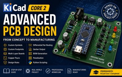
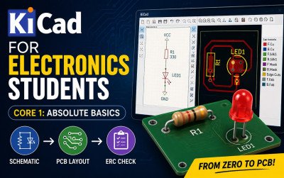
You will begin with KiCad PCB design, learning how to create schematics, work with component libraries and custom symbols, develop PCB layouts, assign footprints, perform Design Rule Checks (DRC), and generate Gerber files. The course then moves into digital logic foundations, covering number systems, binary and hexadecimal representation, two's complement, Boolean algebra, logic gates, combinational circuits, sequential logic, flip-flops, registers, and finite state machines.
The next section introduces Verilog HDL, including module structure, data types, ports, combinational and sequential logic, finite state machines, testbenches, waveforms, and a complete UART transmitter project.
Finally, you will work with AMD/Xilinx Vivado Design Suite, learning project creation, source management, synthesis, implementation, timing analysis, XDC constraints, and bitstream generation. XDC constraints are used to map Verilog ports to FPGA package pins and define timing requirements.
The course concludes with bitstream generation and report analysis, including utilisation, timing, DRC, power, clock interaction, and methodology reports. You will learn how to interpret the critical path and understand whether your design meets timing requirements.